PCB Fundamentals 2: MOSFET Transistors
This post is part of the Senseo series:
- Senseo Prelude
- Senseo Electricity Basics 1
- Senseo Electricity Basics 2: Generation
- Senseo Electricity Basics 3: Grid to Wall Socket
- Senseo Boiler: Heat and Electricity
- Senseo Boiler: Sensing Temperature
- Senseo Boiler: Sensing Temperature Part 2
- Senseo Boiler: Safety
- Senseo Boiler: Brewing
- What is Plastic?
- PCB - Printed Circuit Boards: Fundamentals 1
- PCB Fundamentals 2: MOSFET Transistors
- PCB Fundamentals 3: CMOS Logic
- PCB Fundamentals 4: Combinational v Sequential Logic
- PCB Fundamentals 5: D-Latch
- PCB Fundamentals 6: Clocks & Flip-Flops
- PCB Microcontroller Subsystems: CPU core
- PCB Microcontroller Subsystems: GPIO
- Senseo GPIO Button Example
- PCB Microcontroller Subsystems: ADC (Conceptual)
- Senseo Interlude: Considering Quality
![]() I mentioned that MOSFET transistors are the reason this chip can achieve so much yet be so small. Now a MOSFET is like a tiny switch. It has three legs where drain and source connect two parts and gate is the pin that controls whether drain and source are connected inside. Depending on the type of MOSFET (take NMOS as the example here), gate being pulled high (1) will create a channel inside between the drain and source and allow current to flow.
I mentioned that MOSFET transistors are the reason this chip can achieve so much yet be so small. Now a MOSFET is like a tiny switch. It has three legs where drain and source connect two parts and gate is the pin that controls whether drain and source are connected inside. Depending on the type of MOSFET (take NMOS as the example here), gate being pulled high (1) will create a channel inside between the drain and source and allow current to flow.
With ‘current flowing’, I don’t mean electrons shooting through the wire like water in a pipe. The actual electrons move very slowly. Instead, the signal propagates as an electromagnetic field through the conductor, causing charges all along the wire to start moving almost instantly.
You might now be thinking, if the MOSFET is this chunky and big as we see here in the visual, how can up to a million fit inside the small MCU from before? Well MOSFETs come in various sizes. What we see in the visual is called a power MOSFET, which is what’s used for handling big components on the PCB such as switching motors, heaters and pumps. In order to do this it needs to withstand tens to hundreds of volts, and so needs a physically larger silicon die, thicker metal layers and generally more robustness inside. Note that this type isn’t used on our Senseo PCB, what you instead see in the first visual of last chapter in the middle of the board, is called a Triac. This is more suitable for bridging DC electronics with AC applications such as the boiler and pump, but more on that later.
On the other hand, we then also have what’s called logic MOSFETs (CMOS transistors). These are the tiny switches inside the MCU, which still range in size but on average are around 65nm (0.000000065 meters). Physically they work the exact same way. The reason these can be so much smaller is because they function solely in the world of DC (3.3-5V) and have way less need for heat dissipation. These are build using photolithography and are responsible for much of the advances in tech today. As you may have gathered, and which will be discussed further on, silicon is an important component of these. In fact, silicon is the key material to make semiconductors, among which MOSFETs, and as such the name “silicon valley” suddenly gets meaning.
I also mentioned that “the microcontroller uses the transistors to switch the output pin to VDD (high voltage) or ground (low voltage)”. An important clarification is that VDD stands for ‘voltage at the drain’, this isn’t a strict interpretation in modern circuits though. We actually just see VDD as the positive voltage supply. In logic circuits (modern CMOS), we’ll see this come back many times. Other type of logic circuits do also exist, such as Bipolar Junction Transistor (BJT) circuits (which use Vcc, not Vdd), but since these are an older type that aren’t in the Senseo nor in many modern appliances, we won’t go into those.
Physical layout
We’ve already mentioned this but it’s worth considering properly. A MOSFET transistor has three main terminals: Drain is where the flow comes in, Source where the flow goes out and Gate is the control deciding whether the flow can happen. The direction from drain to source is not a fixed truth, it can be reversed without any repercusions.
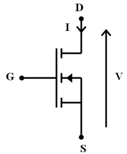 This gate is the part that is insulated from the main pathway by nanoscale glass (oxide), so it can only act as a control switch and not receive or give actual current. This separation results from that very thin insulation layer called oxide, which is actually Silicon dioxide (Silica - SiO₂) which we saw when exploring glass. So the Gate is actually a metal plate that is separated from the drain and source by an oxide (sort of glass). Behind that oxide and in between the drain and source terminals resides the semiconducting silicon itself. In the visual we see how such a transistor is shown symbolically, we may then imagine the oxide to reside in that empty space between G’s metal (vertical full line) and the drain and source parts.
Since gate is a metal plate, the application of voltage to it will make the electric field pass through, but the electrons themselves cannot. For scale, the nanoscale glass insulation that prevents this is about 1-100nm, while a human hair is 80.000nm. Current is blocked by this Oxide, but the electric field that passes through will push or pull charges inside the silicon below. This silicon is the semiconductor, meaning that depending on this push or pull because of the electric field, it will be a channel that opens or closes. We’ll see this in more detail down below.
Metal Oxide Semiconductor Field Effect Transistor
MOSFET itself stands for Metal Oxide Semiconductor Field Effect Transistor. That’s a handful, but becomes quite straightforward once dissected. We’ve seen ‘semiconductors’ before, they’re just special materials like silicon that allow conduction or insulation depending on conditions. ‘Oxide’ is a very thin insulation layer of silicon dioxide (SiO₂ - extremely thin glass) that sits between gate and the semiconductor (silicon). The word ‘Field’ meanwhile comes from the fact that an electric field (voltage) controls whether the transistors switches on or off.
This is then also where it gets interesting. Chemically, silicon contains two types of carriers: electrons (-) and holes (positive missing electron spots), very similar to the diodes we saw before. Depending on how the silicon is chosen to be used (called ‘doped’), it will have mostly electrons (N-type) or mostly holes (P-type). We should imagine here that we have a bunch of people and chairs, and when everyone sits down, there are still chairs left open, those are the holes. So when electrons (humans sitting) move, the holes change places as well. Now the electric field communicating with the silicon can push negative charges and pull positive charges (holes). We can already see where the semi conducting behavior comes from. When an electric field is present, the make of the material changes. And the make of the material in this case are electrons.
That’s what leads us to the two different types of MOSFETs, PMOS and NMOS.
PMOS & NMOS
Conceptual Understanding
Since silicon can be doped in multiple ways, we formally recognize two versions for our transistors.
PMOS: In this case the silicon is P-type, meaning that the main charge carriers are holes. A hole is a missing electron that behaves like a Positive charge, so we can think of this material as having positive charge carriers.
NMOS: Here the silicon is N-type, where the main charge carriers are electrons. Electrons carry a Negative charge, so in this material the current is mainly carried by negative charge carriers.
The big idea now is that Negative charges (electrons) are attracted by positive voltage while positive charges (holes) are attracte by negative voltage. A voltage being positive or negative merely depends on the reference point, so where we start from. This might sound quite vague, but voltage is never absolute, it’s always measured against a reference point.
If we have for instance Gate = +5V and Source = 0V, then source is the reference and gate is a positive voltage relative to the source. But if we then have Gate = 0V and Source = +5V, then voltage at the gate is -5V relative to source. This is actually particularly relevant in our MOSFETs because the only thing we really care about is the difference between terminals, with emphasis on gate and source:
- Vgs = Vgate - Vsource
If Vgs > 0, gate voltage is positive relative to source, and vice versa. The exact specification still depends on the tyep of transistor though.
For an NMOS transistor, the main charge carriers are electrons. When the voltage at the gate is sufficiently higher than the source (above a threshold), an electric field is created across the insulating oxide. This field attracts electrons towards the surface of the silicon, forming a conductive channel between source and drain. In that sense, a kind of “bridge” is created that allows current to flow. Put differently, NMOS conducts if Vgs > 0.
For a PMOS transistor, the main charge carriers are holes. Here, conduction occurs when the gate voltage is sufficiently lower than the source. The electric field in this case attracts holes towards the surface of the silicon, again forming a conductive channel between source and drain. Here we have conduction when Vgs < 0 (gate is negative relative to source).
In both cases, it is not the absolute voltage that matters, but the voltage difference between the gate and the source. Only when this difference exceeds a certain threshold does a channel form and the transistor turns on. This threshold is purely a physical feature of the material, say for instance 0.3-0.8V. The difference between gate and source needs to exceed this in order for a channel to be created.
Physical Understanding
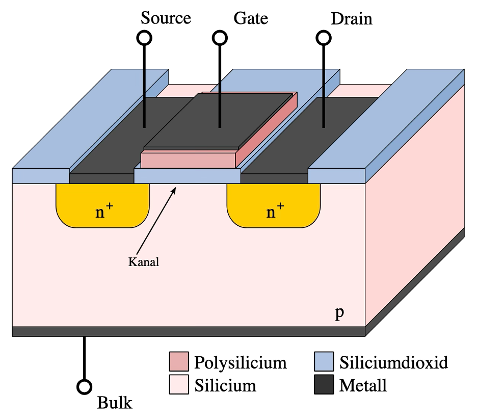 To move this conceptual understanding to a physical understanding, I found the picture on the right that signifies an NMOS type transistor. We can see this by the fact it has an N+ type source and drain, and a P-type body in between.
This is then the next step in our mental model. NMOS actually has a P-type silicon body, while the two terminals drain and source have little embedded N-type regions. Although the body is P-type, it is called an NMOS (N-channel MOSFET) because when it turns on, an N-type channel is formed and current is carried by electrons. The situation we essentially start with is [N | P | N]. No current can flow, and so the transistor is off. When we now apply a positive voltage to the gate, an electric field appears across through the oxide (nanoscale glass) layer, pointing downward, which causes positive charges to repel which leads to a depletion region. Electrons from the N regions are then attracted and as Vgs keeps increasing, more electrons gather at the surface than there are holes still present. This leads to an inversion layer, despite the bulk of the body being P-type. And so we have an N-type path between drain and source that conducts electricity.
PMOS is essentially a mirror image of this. It has an N-type body, and two P type regions and source and drain. We start with a situation where [P | N | P] and no current can flow between P and P because the N-type regions blocks conduction. Now when a negative voltage applies, so when gate has lower voltage than source, then gate actually becomes negative compared to the silicon. This leads to an electric field being created in the opposite direction than before. The electric field is now pointing upward to the gate itself. Because of the negative gate, electrons near the surface are repelled from it and a depletion region forms. When the negative voltage becomes even more negative, the positive charges (holes) from the P regions at drain and source get attracted to the surface, and an inversion layer again forms. Once this happens a path is formed and current can flow.
I realize it might not be intuitive that gate can have lower voltage than source, but this will become much clearer and obvious when considering logic circuits.
Aside on Silicon
Small aside on Silicon: This semiconductor is much used in electronics, and is actually also made of sand (Silica, SiO₂). They start with very pure silica sand, which is mixed with carbon (e.g., wood chips or coal) and heated in an electric furnace at 2000 °C, causing the following reaction: SiO2 +2C→Si+2CO.
Essentially the silicon element is separated and therefore purified (98% so, called metallurgic silicon). Then, something called the Siemens process is performed to convert this into even purer silicon. The metallurgic silicon is turned into a gas by reacting it with hydrogen chloride (Si+3HCl→SiHCl3 +H2). As such we obtain tri-chlorosilane (SiHCl3). This is then heated in order to get out the impurities (which all have different boiling points). Tall reactors then have U-shaped rods in them, made of polysilicon of prior runs having been melted/casted, and these rods are being electrified, creating heat (1000°C) through resistance (just like the boiler from before). This heating in the reactor decomposes the tri-chlorosilane gas we’ve made into a new solid silicon (SiHCl3 +H2 →Si (solid)+3HCl).
The (new) silicon is deposited onto the rods, making them thicker and very pure polysilicon rods. These rods are as such placed in the reactor as a starting point. Apparently the resulting polysilicon rods are many small crystals fused together, while electronic chips require a perfect continuous crystal. Manufacturers therefore kind of ‘regrow’ the silicon, by for instance the Czochralski method. I’m eager to go down this path, but feel I would digress too much. The end result is just a giant single crystal silicon that can be sliced and used for electronics. That’s the semiconductor we find inside the MOSFET.