PCB Fundamentals 3: CMOS Logic
This post is part of the Senseo series:
- Senseo Prelude
- Senseo Electricity Basics 1
- Senseo Electricity Basics 2: Generation
- Senseo Electricity Basics 3: Grid to Wall Socket
- Senseo Boiler: Heat and Electricity
- Senseo Boiler: Sensing Temperature
- Senseo Boiler: Sensing Temperature Part 2
- Senseo Boiler: Safety
- Senseo Boiler: Brewing
- What is Plastic?
- PCB - Printed Circuit Boards: Fundamentals 1
- PCB Fundamentals 2: MOSFET Transistors
- PCB Fundamentals 3: CMOS Logic
- PCB Fundamentals 4: Combinational v Sequential Logic
- PCB Fundamentals 5: D-Latch
- PCB Fundamentals 6: Clocks & Flip-Flops
- PCB Microcontroller Subsystems: CPU core
- PCB Microcontroller Subsystems: GPIO
- Senseo GPIO Button Example
- PCB Microcontroller Subsystems: ADC (Conceptual)
- Senseo Interlude: Considering Quality
CMOS
We’ve now seen the most important building block for most of the electronics in our Senseo machine, so the next step is to explore how it’s utilized so effectively. We’re therefore in the world of CMOS logic, and are still operating inside the brain of the machine, the MCU.
CMOS stands for Complementary MOS (metal oxide semiconductor). But what does complementary mean in this context? Well as we’ll see more formally for the inverter, in every logic gate we use, we implement both PMOS and NMOS. These work in opposite directions, A high gate (input) turns one transistor on while turning the other off. We could then have a series where we have a power source which connects to one of these transistors, and that one is then connected to another transistor, whose other end is tied to ground. This ensures that only one path conducts at a time, because if the input is high (or low) only one of those two transistors will conduct.
The middle point, where the two transistors connect to each other, can then be used as an output node. This is because when we have our input going into this circuit, the output will be either high (1, when connected to the power rail) or low (0, when connected to ground).
This is why CMOS is so preferred in practice. The combination of both PMOS and NMOS turns logic circuits into a very low static power consumption. Power is almost never dissipated directly from the power rail to ground, except very briefly during switching. This is the major improvement CMOS then has over older designs such as RTL with BJT transistors. It’s energy efficient.
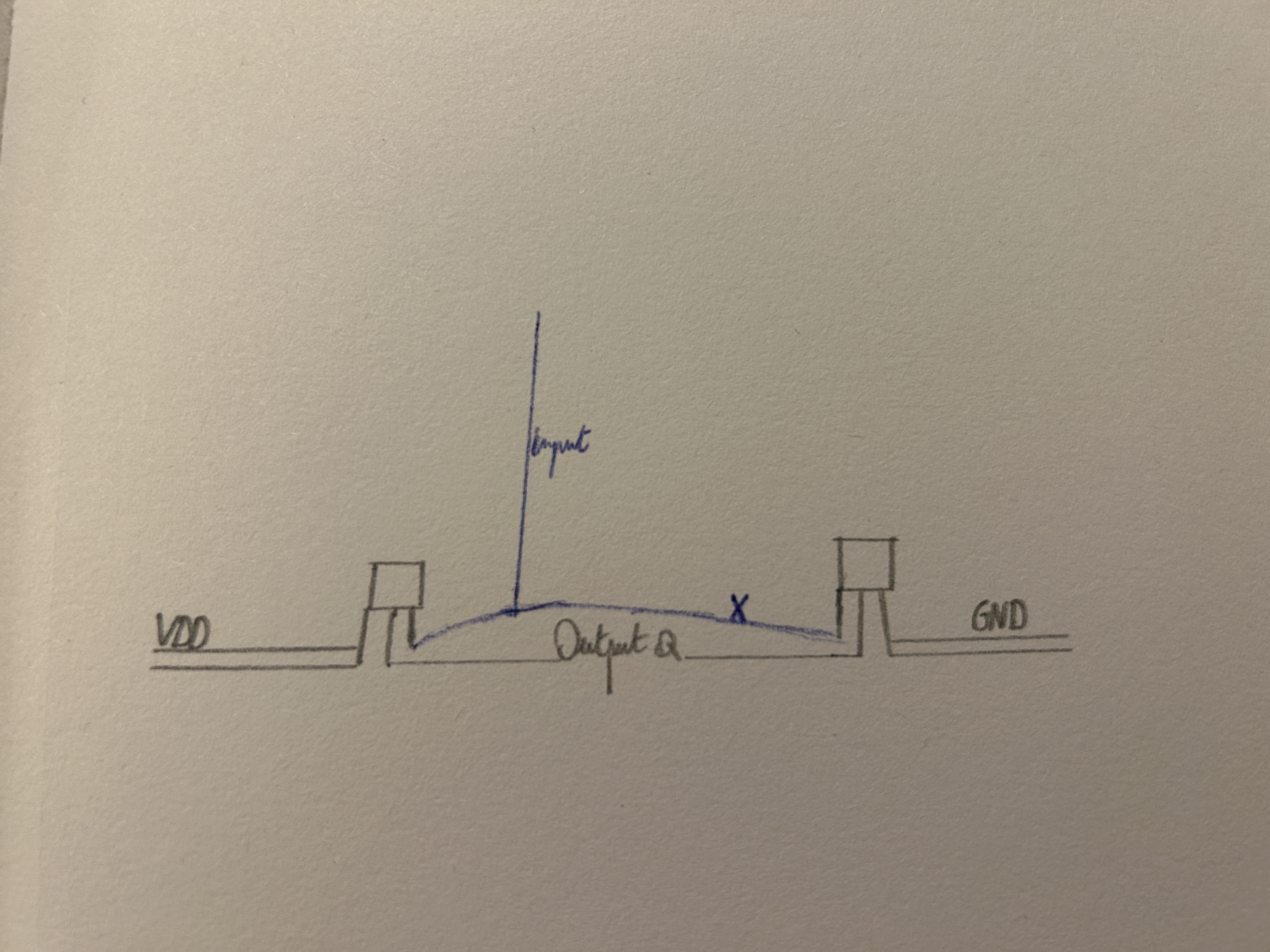
Inverter - NOT gate
The inverter is actually the building block for most other logic gates and truly lies at the basis of even the more complex electronic components of the MCU we’ll see later on. The idea is that if we have an input of say 0, the output will be 1, and vice versa. If we now formalize the above explanation of a little circuit with two different transistors, we arrive at the following:
VDD - PMOS -output- NMOS - GND
VDD historically refers to the supply voltage (originally the drain supply in MOS circuits), but in modern usage it simply means the positive power rail.
GND is ground, but note that this isn’t really a connection to the earth/ground pin in the wall socket. Voltage only works in terms of reference points. If we say something is +5V, it is only so relative to a certain reference point. We saw this in batteries, and also in the consideration of the MOSFET. It’s the same idea here. Ground on this logic gate is merely a point we choose as a reference. It is simply another node of the power supply. You can view this like the use of sea level as the reference point where we say height is 0.
Our PMOS transistor is tied to the power rail, and forms the pull-up path. On the other side, we then have NMOS tied to ground. In the middle of the two, where the pins of PMOS and NMOS connect, is the output node. It is the node where we could measure the output voltage with a multimeter.
Now the reason why we put PMOS against power and NMOS against ground, and not the other way around, becomes quite intuitive if we consider the way each of these works. Remember that PMOS only turns on if Vgs < 0, meaning that voltage at the gate is smaller than voltage at the source terminal. It then becomes convenient that a power supply puts the source terminal at a constant higher voltage. So when input is low (gate 0) the source is necessarily higher, and the PMOS conducts. This is the situation that naturally leads to ‘negative’ voltage, and subsequently to the electrons being repelled from the surface and holes being attracted - having the path (little bridge) formed.
Similarly, NMOS turns on if Vgs > 0. With NMOS against ground, source is always low. And so when input is high (gate 1), voltage at the gate is necessarily higher than voltage at the source terminal. And so the NMOS conducts. This is called the pull-down path, as it pulls down the output to ground whenever NMOS conducts.
Do note that the gates of both NMOS and PMOS are tied to the same input. There’s actually an external little path between the gates in order to make it more efficient and just have the input wire connect to on input node (call it X).
Now all put together, we can consider two states:
- Input high: When input is high, NMOS conducts while PMOS doesn’t. So output will be pull down to ground. An input of 1 leads to an output of 0.
- Input low: when input is low, we have PMOS conducting and NMOS not. As such, output will be pull up to VDD. An input of 0 leads to an output of 1.
Bits and Physical Voltages
Something that might be worthwhile to point out is that voltage being high or low is denoted as the data signal, the binary digit (bit) being 1 or 0. In data language, there’s no such thing as 0.8 or 0.33. Instead, we consider 0-0.8V as a 0 bit, and 2-3.3V (or 5V) as a 1 bit. The middle region is undefined in digital sense, thereby ensuring a sort of noise margin.
No physical object can actually sense these strict 0 and 1’s. These are purely human convention and refer to low or high voltage. In software we use them, but in physical objects everything is continuous. When I refer to output or input being 1/0, do note then that this is my interpretation, and in reality it just means the voltage there is high or low.
The inverter actually helps straighten out a jittery input, as it pulls the output either strongly to VDD or to GND. Because everything is continuous, we actually have that NMOS and PMOS gradually turn on as voltage rises/falls. The consequence of this is that there is a switching threshold at a certain point when PMOS has gradually been turning off while NMOS has gradually been turning on. We usually say this occurs at VDD/2, so either 3.3V/2 = 1.6V or 5V/2 = 2.5V. These aren’t hard thresholds, just the place where the pull up and pull down paths are equally strong (and PMOS/NMOS both partially conduct), and therefore the output node will switch states at exactly this point.
But now remember, if it switches at 1.6V (or 2.5V) how will it be detectable for a next gate (say another circuit attached to our output)? Because here we have signal 0 be defined at 0-0.8V and 1 as 2-3.3V, but 1.6V is perfectly in between? In theory this is indeed correct and unstable, but what actually happens is that transistors have a very high gain around their input. This means that even the tiniest change in input leads to pretty remarkable changes in the output. So it’s never really a problem. When we move to memory we’ll see that this can lead to metastability, but that is a problem for later.
AND Gate
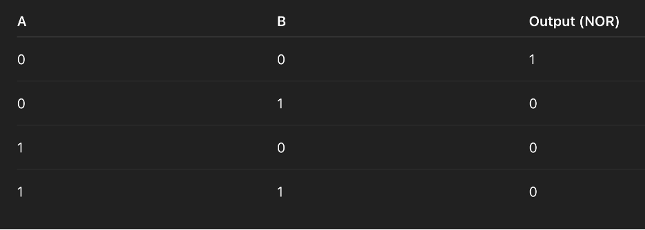
Now for the AND & OR gates, it must be noted that CMOS actually creates NAND & NOR more effeciently.
Starting with NAND, the idea is that we now again have a pull-up and pull-down path but this time with four transistors in total. NAND is simply that output is 0 only if A and B are 1. Intuitively this makes sense, NOT(AND) reverses the AND logic, and AND dictates that output is 1 only when both the input nodes are 1.
What we therefore sense here is that we don’t have one single input node anymore. Of these four transistors, pairs are connected via their gates so as to have two separate input nodes, A and B.
VDD = PMOS (A) = PMOS (B) = Output - NMOS (A) - NMOS (B) - GND
Note that ‘=‘ refers to being parallel, while ’-’ refers to being in series. PMOS here therefore has A and B both connected with one side to VDD and another to output. For the rest, we see that:
- For the pull-down path (NMOS - on if input 1), we want to have a connection to GND only if A and B are both on (input 1), which is achieved by having two NMOS in series. If both are receiving high voltage at their gate, both are on and output is pulled to 0. If either A or B has input 0, the output won’t be pulled low (0).
- The pull-up path (PMOS - on if input 0) then has the goal of connecting power to output when either A is 0 or B is 0, or both. As such two PMOS transistors are put in parallel so that if A has input 0, PMOS(A) is on and output is 1 and similar for B. Only when both A and B have input 1 are both PMOS off.
The goal for this NAND gate is to be aligned with the following truth table:

After achieving the NAND result, we simply connect the output node of the NAND gate to the input of a NOT gate. This results in getting the exact opposite behavior of the NAND, which is evidently the AND gate. When the NAND output is high, the NMOS in the inverter is turned on and there is a connection to ground (0). When output of NAND is 0 (meaning both A and B have input 1), the PMOS on the NOT gate will turn on while NMOS is off, and output of the inverter is also 1. It’s tricky but intuitive.
OR gate
Lastly, for the OR gate we again start with the NOR logic and work our way to OR. The NOR gate again works with the A & B input nodes logic, such that output of NOR is only 1 when both A and B have input 0. If either A or B has input 1, output becomes 0. The full path now looks like
VDD - PMOS (A) - PMOS (B) - output = NMOS(A) = NMOS(B) = GND
Such that now PMOS connecting to VDD fall in series while NMOS is parallel with both A and B connecting to output and GND. On the NMOS side (pulling down to ground), the idea is that we get the output low (0) if either A or B has high input (1). Meanwhile with the PMOS side (pulling up to VDD), we allow output to be high (1) only if both A and B are off (0).
We therefore achieve in aligning the output with the NOR truth table:
If we now again connect the NOR output to a CMOS inverter, we flip it and get the usual OR gate.