PCB Fundamentals 6: Clocks & Flip-Flops
This post is part of the Senseo series:
- Senseo Prelude
- Senseo Electricity Basics 1
- Senseo Electricity Basics 2: Generation
- Senseo Electricity Basics 3: Grid to Wall Socket
- Senseo Boiler: Heat and Electricity
- Senseo Boiler: Sensing Temperature
- Senseo Boiler: Sensing Temperature Part 2
- Senseo Boiler: Safety
- Senseo Boiler: Brewing
- What is Plastic?
- PCB - Printed Circuit Boards: Fundamentals 1
- PCB Fundamentals 2: MOSFET Transistors
- PCB Fundamentals 3: CMOS Logic
- PCB Fundamentals 4: Combinational v Sequential Logic
- PCB Fundamentals 5: D-Latch
- PCB Fundamentals 6: Clocks & Flip-Flops
- PCB Microcontroller Subsystems: CPU core
- PCB Microcontroller Subsystems: GPIO
- Senseo GPIO Button Example
- PCB Microcontroller Subsystems: ADC (Conceptual)
- Senseo Interlude: Considering Quality
We’ve now seen quite a few basics, from combinatorial logic where basic circuits create a stable equilibrium dependent on current states, to memory and the way latches are used to overwrite it. Latches were the way we could choose which value to freeze and store for later. Now as we saw at the end of last blog, the insufficiency of latches comes from the lack of controlled progression, as they keep copying as long as the enable wire allows them access to the memory block. What we’d instead like is a system that changes in clean and countable steps, and not as long as signals are allowed to flow. Because of this insufficiency, we had the problem that the outcome was mainly dependent on physics details and not logic structure itself.
As such, the concept of a clock is introduced, to control when the system is allowed to change states. It’s not a memory creator, but a device to control when it may and may not change. We essentially now introduce time itself into the picture. Physically we have a circuit that oscillates, meaning it produces a voltage that repeatedly goes high and low (0V → VDD → 0V → VDD → …). In microcontrollers this is most often a crystal oscillator (Pierce oscillator). The idea is that they consume power and continuously toggle a wire between GND and VDD. A clock is then placed in the microcontroller and wires to every element that stores states. On the memory block we’ve seen before (cross-coupled inverters) it connects to the input, which in modern digital design means the flip-flop’s enable input wire (not just a d-latch - see later).
Now physically this is likely one of the most impressive elements we’ve seen. A crystal oscillator is literally made with sand (chemical compound silica), but more precisely quartz. Quartz is then a mineral (specific crystalline form) made of silica. The sand we find on the beach is most often tiny broken down quartz crystals. Now quartz has a unique property called piezoelectricy, which implies that mechanical stress slightly shifts the internal crystal structure. Such shifting in turn causes positive/negative charges to separate and in turn creates voltage. Similarly, if we apply an electric field to it (such as power inside the microcontroller), the quartz crystal deforms slightly and oscillates at a very precise and repeatable frequency (same idea is what powers the quartz watches). In fact, a lighter’s spark is similarly produced by the spark of a piezoelectric crystal. For a great guide on the oscillator.
VDD doesn’t power the crystal directly, instead it powers a small amplifier circuit made of transistors which is then connected to the crystal and produces a loop of activity. This amplifier is a single CMOS inverter, but where the two transistors are rigged in such a way that they become an amplifier. Where we normally have it so that if input = 0, output = 1 and vice versa, we now have it so that input is forced to sit halfway between 0 and 1 (at the threshold). This way, where PMOS and NMOS are both partly on, output becomes very sensitive so that a small input change leads to big output changes. The inverter therefore becomes a voltage booster instead of a logic gate. The input of the inverter is then connected to the quartz crystal and a few tiny capacitors (remember the buckets allowing more consistent flow).
When power is turned on, physically electric fields appear everywhere and the MOSFETs in the amplifier become able to conduct. Now because of the biasing of the transistors the input as also pulled about halfway to VDD such that the inverter is in a very unstable state. Now because of this instability, even random noise becomes meaningful, and the universe isn’t quiet. There are random electrons moving everywhere (called thermal motion). The capacitors trap these charges and release electrons, which causes microscopic voltage fluctuations on the inverter input. Nothing would happens if it was at absolute 0, but through the rigging even nano volts have influence. Now nothing from the power supply is attached to the crystal, so still we might wonder how it can start doing anything? Well the crystal is attached to the inverter input and when that input starts jittering because of nano volts, that same jitter starts appearing across the crystal electrodes (the conductor through which electricity enter/leaves and object). As such, an electric field appears in the crystal, not a meaningful one but physically it’s there. Now because the input charge is near threshold, any tiny change causes a larger output change, such that nanovolt in the input becomes microvolts at the output, which is fed back to the crystal. As such the loop starts, but the frequency is still random. This is where the magic properties of the crystal piezoelectricity comes in, as it responds especially strongly at one exact frequency and as a result the noise at the crystal’s frequency get amplified. One vibration is therefore what survives as the inverter specifically amplifies that one.
We’re now at the stage where the crystal is physically oscillating (bending back and forth) thousands/millions of times a second at a fixed frequency. This mechanical motion creates an alternating voltage on the crystal terminals. Now naturally because of the nature of the amplifier, the oscillation will keep growing until the inverter physically cannot amplify more (due to transistor limits) and the result will become that energy added per cycle = energy lost per cycle —> a stable oscillation. Now a mechanical rule that is similar for a pendulum, guitar string and here the quartz oscillation is that any physical object that vibrates freely prefers to do so in a sinusoidal motion (the sine wave we saw in high school), which gives us the purest possible time reference due to its stability against noise. Now because of the piezoelectric property, sinusoidal mechanical motion leads to sinusoidal electric voltage.
As you might recall from the battery section, there is a slight difference between electrodes and terminals, where the electrode is the conductor (material allowing flow of charge) while the terminal is an external connection point to the circuit. That’s the same here with the quartz crystal. A small metal wire is attached to the terminal of the crystal and because of the oscillation there is a voltage on it going smoothly up and down. But we don’t have a clock yet. We’re currently in a position where since waves go up and down, meaning it spends time in between 1 and 0, which makes it ambiguous for logic. We therefore want to convert it into square waves.
How do we do this? Well very simply, we attach the wire coming from the crystal’s terminal to another inverter (called here a ‘buffer’). This time it’s a regular inverter without rigging, where the input voltage increases and once it crosses the inverter’s threshold voltage (part of the design), NMOS suddenly turns on and PMOS off, such that the output snaps from high to low. As such we get a fast electrical transition without ambiguity. This is then the clock edge, which is simply the moment the inverter switches. We then have a rising edge (output low —> high) or falling edge (high —> low).
Essentially, the clock is the first element seen by power in the microcontroller. When power is applied, the oscillator directly starts oscillating, which spreads the clock signal then through the chip and on each clock edge the flip flop updates (as well as other elements we’re not going to put under a microscope) and between clock edges we then have that combinatorial logic settles and no memory is allowed to change. As such we have compute - freeze - compute - freeze
We then also have flip-flops as essential upgrades of the d-latch to force change only once per cycle. With the D-Latch we had the problem that memory could keep changing throughout one cycle as long as there was transparency (EN on). Now a D flip flop is essentially a tiny circuit copying one wire (D) into the memory cell exactly once, when the clock edge happens, and then refuses to change until the next edge. So it samples once and then holds firm (no leakage). Now physically it’s built from two D-latches, inverters, transmission gates and the clock wire.
Now when we talked about the D-latch earlier, we actually referred to the cross coupled inverters plus the transmission gate (something allowing transparency at times), it was the whole block. For the flip-flop we can imagine the big picture to look like
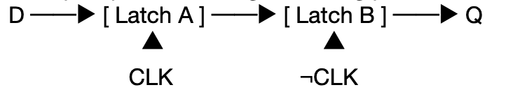
 Where each latch block has a cross coupled inverter (memory) and a transmission gate. Essentially we have two versions of the figure I drew earlier attached to one another. Both A and B are full latches, with the difference between them being when they’re allowed to change. So essentially in this view, which is getting quite intricate, we have our information wire D coming to the transmission gate of latch A just as with the D-latch. Then a metal wire is attached to the output node of latch A (Q or Q̅) and goes to latch B’s transmission gate, which has no D wire but just the wire coming from A. Then B is also again just the D-latch from before. The only other difference, as my little diagram indicated, is that the enable (EN) signal wires are replaced now with clock edges CLK and ¬CLK (‘not CLK’), but functionally the idea remains the same: CLK = 1, latch A is transparent, 0 it holds; while for ¬CLK there’s again an inverter attached to CLK, so when CLK = 0, ¬CLK = 1 and vice versa.
Now we also see that when latch A is open (CLK), B is closed (¬CLK), meaning that there’s never a moment when D coming into the flip flop and the output Q are fully connected. This is why data cannot just flow through as before, and only one transfer happens per clock edge. Really quite clever. So A captures the data first, B captures that capture in turn, and then holds it for the rest of the cycle. The output of the second latch is then the architectural state (Q). So what we finally see is our signal D being allowed entry when the clock edge is on CLK = 1, and then when the clock edge turns off (falls), that signal gets access to latch B, and Q holds the new value. One state change per cycle is achieved.