PCB Fundamentals 4: Combinational v Sequential Logic
This post is part of the Senseo series:
- Senseo Prelude
- Senseo Electricity Basics 1
- Senseo Electricity Basics 2: Generation
- Senseo Electricity Basics 3: Grid to Wall Socket
- Senseo Boiler: Heat and Electricity
- Senseo Boiler: Sensing Temperature
- Senseo Boiler: Sensing Temperature Part 2
- Senseo Boiler: Safety
- Senseo Boiler: Brewing
- What is Plastic?
- PCB - Printed Circuit Boards: Fundamentals 1
- PCB Fundamentals 2: MOSFET Transistors
- PCB Fundamentals 3: CMOS Logic
- PCB Fundamentals 4: Combinational v Sequential Logic
- PCB Fundamentals 5: D-Latch
- PCB Fundamentals 6: Clocks & Flip-Flops
- PCB Microcontroller Subsystems: CPU core
- PCB Microcontroller Subsystems: GPIO
- Senseo GPIO Button Example
- PCB Microcontroller Subsystems: ADC (Conceptual)
- Senseo Interlude: Considering Quality
Now that we can build logic gates, the next question is: how do we use them to make useful decisions and computations? We’d like to have a machine react to inputs and perform the correct actions resulting from those. Now with CMOS we have a really powerful ingredient. We can wire things in such a way that the output voltage is a function of input voltages. That’s the logic gates resulting from arranging PMOS and NMOS, which are essentially just doing Boolean algebra.
Combinational logic and Arithmetic circuits
Combinational logic is a type of logic where the output only depends on the current inputs. It’s the logic we’ve been in up till now. When there’s a change in input at a given moment, that change is translated to the output almost instantaneously. This might seem self-evident, but there’s another type of logic that introduces the idea of memory and the notion of time, called sequential logic.
As a result, within this logic family, we could build and structure our logic gates in such a way where the output is a function of inputs [y=f(x)]. Essentially based on our boolean gates we could mimic basic algebraic formulas, including adding, subtracting, comparing, selecting and so on. This is also where the idea of a calculator came in historically, through transistors and logic gates.
I realize this is quite abstract still, but consider the truth table, which we saw for instance for the NAND gate in the last post. Based on a complex circuit of transistors that are merely puzzled together in a certain combination, we can derive a logical and consistent result. We get sort of rules about what input combination leads to what output. So when we know what kind of output we want, we can work ourselves backward and see which combination of inputs is needed. That’s the big idea of combinational logic, which we’ll here explore for the most basic arithmetic example of ‘addition’.
Addition
As mentioned, when we know what kind of output we’d like to have, we must work our way backward to see which combination of inputs is needed for it. What is first needed here, though, is a little recap on what addition actually is.
Decimal Addition
The usual addition we’ve all known and learned in school is the decimal one. It’s what we use in everyday life by counting on our hands if necessary.
Now this is quite far in memory but in kindergarten math we encountered the notion of a “carry”. if we want to add for instance 156 and 155, we place them above each other and go number by number. Since 5 and 6 add to 11, we have the carry the one to the next addition of 5 and 5 (and then again to the next).
What we’re then using is a base-10, where we use numbers 0 to 9 and multiply with 10 to a certain power. This idea comes from the decimal place value chart:
[Thousands|Hundreds|Tens|Ones|.|Tenths|Hundredths] [10^3|10^2|10^1|10^0|.|10^-1|10^-2]
Each position in for instance 156 is then represented as a power of 10, so 1 * 100 (10^2 since two places left of the ones), 5 * 10 (10^1), 6*1 (10^0). The general rule is digit × (base^position).
We then have rules such as the carry, where if we add two numbers that go beyond the 0-9 values that are possible in a certain position, we carry that to the next position. 9 + 1, which is 9 * 10^0 + 1 * 10^0, would’ve become 10 * 10^0, but there is no place, so we carry and denote as 1 * 10^1 = 10.
Binary Addition
The same idea now holds for our binary system, which we need to represent bits using voltage as signal. We’re now not in a base-10 system but instead in a base-2 system.
Logically nothing changes really. Each position can now hold values 0 to 1 instead of 0 to 9, and our positions aren’t determined by powers of 10 but instead powers of 2.
[Eights|Fours|Twos|Ones|] [2^3|2^2|2^1|2^0|]
A binary 1 0 1 is therefore 1 * 2^2 0 * 2^1 1 * 2^0 = 4 + 0 + 1 = 5. It’s a little tricky to wrap the head around, but still quite intuitive.
Similar to before, we have a carry rule. Instead of 9+1 giving 10, we now have 1+1 needing a carry and becoming binary 1 0. We can therefore already see some basic notations:
- 0+0 = 0
- 0+1 = 1
- 1+0 = 1
- 1+1 = 10
Everything else comes from the carry propagation.
Each bit position then represents a wire, and so we arrive at for instance a 4-bit (base 2) number as 4 wires, such as for instance 0100 (1 * 2^2) which is 4. Doing some math, the max value such as 4-bit number can take is 15, which is quite small. Now since these 4-bits really are just wires, we can easily scale this. An 8-bit has max value 255, a 32 bit 4 billion, and 64-bit such as a modern laptop up to 18.4 with 18 digits behind it (quintillion?).
Logic Representation
Since our Senseo electronics are only able to represent the binary 0 and 1 through voltage, we naturally fall into base-2 binary addition. Now each position will be represented by a wire, but some more ingredients are needed to accurately represent the carry system. This leads us to the natural combination of a XOR gate and the AND gate, whose joint output is capable of the job.
We already saw the OR gate, but there we had it that output is high (1) if either A or B is high, or both. So the moment just one of them is on, output = 1. Now with XOR we get the Exclusive OR, meaning that output is only 1 whenever A or B is 1, but not both.
Now if we want to add 2 bits, which is the simplest case of hardware/binary addition, we’d get the following truth table:

The sum column we can easily recognize as actually being just an XOR gate, while the carry can actually easily be represented by an AND gate. This carry (AND gate) then represents information not fitting the current bit position. The hardware has no idea it’s summing or carrying, though, that’s just our interpretation. Like we said before, we know what output we’d like, so we work ourselves back to ensure the inputs align.
And just like the above truth table displayed, we now arrive at the wish to add two inputs A and B. We also saw that the whole mechanism of carrying can be entirely represented by two gates, XOR and AND. All that remains is to formalize the mechanics.
The half adder is actually what we have here. We let A and B flow to a parallel circuit where both are connected to the input of an AND gate and a XOR gate. Intuitively, it makes sense that if neither A or B is high, neither gate will see anything. When A is high or B is high but not both, the XOR gate’s output will represent the one resulting from this. Meanwhile if both A and B are high, the XOR gate’s output will be low (0), but the AND gate’s output will be high (1). And so we get a carry; 1 + 1 = a carry to the next wire (1 0).
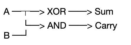
This makes it a ‘half’ adder and essentially tries to answer two questions, whether the voltages are different (XOR) and whether both voltages are high (AND). By having the wires to these gates in parallel, both can be answered and serve to decompose the relation of A with B.
From this we can go to the full adder, because with binary addition when we add multi-bit numbers, each bit position must also accept a carry from the previous position. In a full adder, we then have the sum being the bit that stays in position, and the carry out which is the bit that moves to the next position. As such we have A + B + Carry-in —> (sum, carry-out). Remember the addition of 156 and 155, when we get to the sum of 5 and 5 in the middle, we also have a carry-in from before so must take this into account.
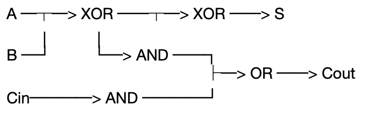
In physical terms this carry-in is just a wire coming from the previous stage. You see, in practice, numbers are often represented by multiple bits. A single bit would only be able to take on two values (that we conceptually interpret from it), namely yes/no, 1/0 etc.
The two-bit scenario with 4 values will have 2 stages. And if we extend the logic of always having A and B inputs, we see the full picture of this two-bit number as:
A0; A1;
B0; B1;
So in stage 0 (A0,B0), we always just have the half adder. The result of this half adder can be either nothing happens (0), a sum happens (simply 1) or a carry in the case of the AND gate being activated. This carry must go to the next stage, where it comes in as a carry-in. We then get to stage 1 (A1,B1), which is a full adder, since the carry in from stage 0 helps conceptualize the prior value. Again, we’ve just looked at what output we desire, and puzzled it together so that the input behaves accordingly.
Now at the last stage, you might wonder, what happens if we must carry again? And that’s a very good question. There is essentially no next stage to carry to, so the adder block usually just has a wire coming out which is seen as a separate output pin, the carry-out. It’s then up to the system designer to make use of this in some way. So after the last stage, here in our two bit example, we’ll see three wires coming out, two sums, and one for carry. In multi bit circuits, however, there’ll be as many sum wires at the end as there were stages/positions, plus the 1 carry-out.
Realistically there are three options at that point, either treat it as a larger number (100 binary), ignore the third wire as carry-out, or connect it to another stage, which is how we can make a 3-bit adder.
And this is how adding works using the hardware we’ve seen. Using the same tools, all kinds of other operations can be handled, such as subtraction, comparison, absolute values, multiplication, division and so on. They’re not super straightforward and I’m interested to explore, but I’d digress too much.
Sequential logic
Now combinational logic has no memory, which means that only current inputs have an impact and that once inputs stop changing, the circuit settles to a fixed state. But what now if we want to count how many times a button is pressed or have steps going in the right order? That’s the reason we want a circuit whose output depends on the past and not exclusively on the present.
Such a sequential circuit then has an internal state, meaning something created in the past influences the present. It persists even when the input doesn’t change. The simplest possible question is how we can store just one bit? Well apparently CMOS is quite elegant for this in that if we feed output of a CMOS gate into its own input, the circuit remembers.
Remember the NOT gate, which had VDD - PMOS - output - NMOS - GND, where PMOS conducts when input = 0, NMOS when input = 1. As such we had high output when input was low, and no direct path ever from VDD to GND, except briefly during switching. Now if we take a wire and connect the output of this inverter gate to its input, then there’s no external signal driving the state of this gate anymore. It’s quite intuitive that the result is that the inverter will just keep flipping its own output, since each change propagates through the inverter itself. Output is low so input becomes low, turning PMOS on and in turn turning output high (and input high), in turn switching NMOS to conduct to ground and turning output low, and so on. This doesn’t yet create memory but it does portray the idea of feedback, which turns a static logic element into a dynamic one. Meaning that a dependence on time and prior values is created.
Now to move from feedback to memory we want a state that reinforces instead of destroys itself. To accomplish this, we simply add a second NOT gate after. We now have inverter A and inverter B, where the output of inverter A becomes the input to inverter B. The output of inverter B then again goes to the input of inverter A. This makes two stable equilibrium points of the circuit, either it’s in high or in low. Say output of A is high, meaning PMOS conducts and NMOS doesn’t, then the input of inverter B is high, causing NMOS on B to conduct and the output of B to be low. Output of B is low, then input of A is low, which causes PMOS to conduct and output of A to be high. As you can see, there’s two stable equilibria possible on the circuit, also called “Bi-stability”.
We’re not yet able to influence what happens, this is just a self-perpetuating circuit at this point, but we can imagine the fact that information is stored as node voltages. The next step is therefore to get external signals to temporarily overpower the feedback, creating a latch. Let’s call the output on inverter A Q, and on B Q̅ (‘not Q’). Now in such a memory cross coupled inverter, we’ll have Q = 1 and Q̅ = 0, or vice versa, because the two continuously reinforce the state in each other. The idea of the latch is to sometimes have this reinforcing dominate (hold the state), and sometimes want a new input to dominate (write).
An intuitive way to do this is via the S-R latch. We basically introduce two new elements, S (set) and R (reset), which are additional transistors that we attach to the output nodes Q and Q̅. It’s actually very intuitive, on both inverters we place an additional NMOS transistor, where input (gate) is coming from elsewhere (whatever is controlling the overriding of the memory). These transistors still connect the output node to ground through source and drain.
Now let’s say the memory needs to be overwritten. Then either S or R will get turned on, and conduct the output of Q or Q̅ to ground. As a result, the output goes low, but then the input of the other also goes low and that PMOS gets activated, turning output high.
You can probably already see an issue with the SR latch, where if both S and R are on at the same time, both outputs go low. The result would be that we don’t know which of the two will overtake the other. We have no idea whether we’ll get Q = 1 and Q̅ = 0 or vice versa. This indeterminacy is an invalid state, which we don’t want. But we’ll see the solution for this next time with the D-latch.
Visually, one of such inverters looks as follows:

In practice, SR latches are often built in a slightly different manner, however, since we might want to actively drive the node high as well as low. We still have two cross-coupled inverters A and B which already have memory and store bits. For a canonical SR latch people then usually cross couple the NOR gate we’ve seen before, as these inherently contain pull-up and pull down without additional forces. However, while still interesting, we’ve got the gist of the SR latch idea.