PCB Microcontroller Subsystems: GPIO
This post is part of the Senseo series:
- Senseo Prelude
- Senseo Electricity Basics 1
- Senseo Electricity Basics 2: Generation
- Senseo Electricity Basics 3: Grid to Wall Socket
- Senseo Boiler: Heat and Electricity
- Senseo Boiler: Sensing Temperature
- Senseo Boiler: Sensing Temperature Part 2
- Senseo Boiler: Safety
- Senseo Boiler: Brewing
- What is Plastic?
- PCB - Printed Circuit Boards: Fundamentals 1
- PCB Fundamentals 2: MOSFET Transistors
- PCB Fundamentals 3: CMOS Logic
- PCB Fundamentals 4: Combinational v Sequential Logic
- PCB Fundamentals 5: D-Latch
- PCB Fundamentals 6: Clocks & Flip-Flops
- PCB Microcontroller Subsystems: CPU core
- PCB Microcontroller Subsystems: GPIO
- Senseo GPIO Button Example
- PCB Microcontroller Subsystems: ADC (Conceptual)
- Senseo Interlude: Considering Quality
Next in the MCU we encounter the GPIO - General Purpose Input Output pins. We’ve seen the CPU, which is essentially millions of flip flops connected via combinatorial logic and driven by a clock. A bit (binary digit) that the CPU understands is one that is synchronized by the clock, lives in a flip flop and has setup and hold constraints. The CPU is kind of like a self contained box when it comes to bit reading. We cannot simply connect wires coming from all places, especially when it comes to components like a boiler which are driven by AC 230V instead of the electronics DC 3V or less.
That’s where the GPIO pins come in, their job is to act as a controlled interface that makes external signals safe and usable for the CPU. It adds input buffers, synchronization latches, optional filtering, output drivers and protection circuitry. It’s a circuit that makes an external voltage safe to turn into a CPU bit. When we for instance push a button on the machine, a wire in the machine drives this to the CPU, but will first stop at a GPIO pin, where an input buffer converts voltage into a logic level. The signal from this is then synchronized to the clock, the value is stored in the flip flop and the CPU then reads that flip flop.
Now what is this synchronization? The clock driving the CPU is pretty self contained in that it has VDD driving a quartz which in turn generates a sine wave, which is turned into a square wave (clean 0 1) with an inverter. The CPU has absolutely no idea when the outside world changes. So how do we safely take a voltage that can change at any time (a button press for instance) and turn it into a clocked bit? The idea here is to wait until the clock edge and then sample whatever voltage is available to be sampled.
Pin MUX
There’s this pin at the edge of the MCU which lets outside systems connect to a certain particular subsystem of the MCU. This pin then feeds just one block and that block decides what the signal means. We therefore have a multiplexer (MUX, the same exact building block as used in the PC of the CPU) that decides to connect the pin either to the GPIO, ADC, timer etc. Note that the GPIO isn’t a filter for the whole MCU, it simply exists to give the CPU (the brain) a generic way to read or drive a pin as a logic value.
Without the GPIO, the voltage the CPU must read would be quite messy. So when the CPU wants to read or drive signals in the machine, it needs the GPIO. For the Senseo machine this comes down to tasks such as driving the brew button and whether the tank is present. These are anything software isn’t, they’re human driven and completely uncoordinated. Same goes for the LED buttons that blink, which are driven directly by the CPU, through the GPIO.
Now in the MCU we have many other components (called peripherals) that also use the pin, such as the ADC (boiler) and the timer (which gets used for pump speed (PWM) and capturing flow sensing). These all share that same pin and the multiplexer selects which one gets connected to the pin at a certain time.
The reason we switch between peripherals when plugging to the MCU connection is that if we’d connect multiple at once, we get a lot of noise. If the ADC were connected together with the GPIO, the Schmitt trigger would inject noise and the accuracy of boiler temperature sensing collapses.
Input Buffer: Schmitt Trigger
So we have an external voltage (e.g. button or sensor) that can change at any time regardless of clock or anything else inside the CPU. This is called an analog voltage. The GPIO then first uses an input buffer (often the Schmitt trigger ~ Dokić type) to clean up that voltage and turn it into logic. This Schmitt trigger comparator turns noisy and imperfect analog voltage into a clean digital 0 or 1. It’s the same Hysteresis concept we’ve seen at the boiler heating. We have 2 threshold, e.g. V-t+ and V-t- where if the noisy voltage exceeds V-t+ (falls below V-t-), the buffer turns it into a clean 1(0).
Now you might think such a hysteresis band would become messy if we have both boiler of 230V and sensors of 3V using it. The thing is however, there is no GPIO anywhere near the boiler, the boiler’s voltage goes through a bunch of places before it reaches a GPIO, where it’s already turned into 3V DC. The electronics world we’re now operating in is purely DC small voltages. What this Schmitt trigger essentially ensures is that a ‘weak’ push of the button and a strong one have the exact same effect in the MCU, so that both elicit the exact same response. Yet despite the boiler’s 230V being leveled down, it’s still extremely volatile and noisy, so likewise it needs stabilizing before being sensed by the CPU.
The Schmitt trigger has the main goal of creating hysteresis, meaning that noisy input only leads to clean output by requiring to pass a certain threshold, both upward (PMOS pull-up) and downward (NMOS pull-down). Now there are many designs used in practice, even without sub-models of design. As such it can get a little tricky getting the mental model exactly right. I’ll focus on the original Dokic design from 1983, as going directly to the source provides the most reliable material. Nowadays, however, this Dokic Schmitt trigger is a little different, and usually uses 6 MOSFET transistors and even some other novel components. But let’s sit with the basics:
We have a main stack of regular CMOS transistors placed in formation like the inverter
VDD - P1 - Output - N1 - GND
But to this stack we add some other components, namely two resistors and two extra feedback transistors. Now as discusses before, such resistors are pretty passive devices, whose sole job is to resist the current coming from the rails in this case. By isolating the inverter source pins from the supply rails (VDD/GND), these resistors allow these source voltages to be modified by the output through the feedback transistors. Without such resistors, the PMOS and NMOS source (see S below) would be clammed hard to VDD/GND. By adding these resistors, internal nodes are created to which these source pins are attached. Visualizing this gives us:
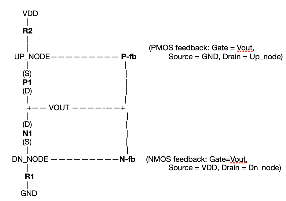
Note that the gates (remember gate, drain, source) of these feedback transistors are tied to the output, effectively providing us a sort of memory feedback in the sense that the output given by the previous state determines the impact of current input. Further, the source of these feedback transistors are tied to the other side’s rail. Don’t mind the drawing, gate is attached to output, source to the other side’s rail, drain to the internal node. Now consider the following:
At a particular moment, we find input (gates of P1/N1) and it is high. This in turn means N1 is on, P1 is off. If N1 is on, that means there is a path to ground and the output has been pulled low. So far so good. Now if output is low, that means the gate of P-fb triggers this feedback transistor on. As such there is a conducting path from GND to the internal upward node, pulling this node low. This has no immediate effect, because with input high, P1 doesn’t conduct anyway. But now consider what happens when input is falling. This means that N1 will gradually taper off, and P1 will equally gradually turn on. But remember that for P1 to turn on, we had that VSG > Vth (V-source - V-gate > internal switching threshold) and we saw that the upward internal node is being pulled to GND. The direct effect of this is that V-source of P1 is near 0V, and we essentially have 0 - V-gate where gate is the falling input (and P1 turns on if input low). The input must therefore fall lower in order to have VSG exceed the switching threshold. So P1 will turn on and pull the output to VDD, but at a biased moment, when when input is lower than it otherwise would’ve needed to be. So now we come to input being low and output having consequently turned high (P1 conducts VDD to output). With output high, P-fb has turned off and N-fb has turned on, resulting in the downward internal node being pulled high. But again nothing happens, because input is low and N1 doesn’t conduct. Whenever input starts rising, however, a similar story takes place. For N1 to turn on, VGS > Vth (V-gate - V-source > internal switching threshold) so that with a source that is pulled high, gate (input) must rise further before VGS is higher than the switching threshold. Whenever that threshold is exceeded, N1 conducts and the output is pulled to GND, switching off N-fb and turning on P-fb. That’s the story of hysteresis. Two thresholds are created through feedback, and noisy switching is preventing.
Synchronization
From the input buffer, we’ve now received a clean 0 or 1 based on the outside analog signals. Before getting this into the MCU, however, we want to synchronize it to the clock edge, so that it plays nicely with the other signals in the CPU core. What’s done in order to achieve this is that the output node of the Schmitt trigger is attached to the input of a flip-flop. And remember from before, the flip flop’s ‘enable’ can be attached to the (same) clock as the other ones in the MCU. So the D flip flop takes in the stable input and synchronizes it to the clock edge.
The major problem is that the rules of the flip flop will be broken through timing. It actually has two rules, namely setup time (input must be stable before clock edge) and hold time (input must remain stable after clock edge). What happens, though, is that the input transition at times happens near clock edge but not exactly on it. This is unavoidable for a GPIO because buttons being pressed, sensors going off and other external clocks all depend on timing, and have nothing to do with the noise cleaning the Schmitt trigger does.
So what happens is that we have our flip flop, which is just two cross-coupled inverters and a few transmission gates, and the clock edge (the enable on the transmission gate) happens when the input is changing. At such a moment, the internal nodes of the flip flop will enter a metastable state because one will try to become 0 and the other 1 (detect the input). This metastability means nothing more than that the output will sit at an intermediate voltage longer than we’d like it to. So not 0 or 1, but somewhere in between, which leads to thermal noise or mismatching at a moment we cannot predict when it will happen. Such metastability will break data paths further on as a result of short glitching or different values in different paths. The worst thing is that it’s a hardware phenomenon, so no software will even detect this.
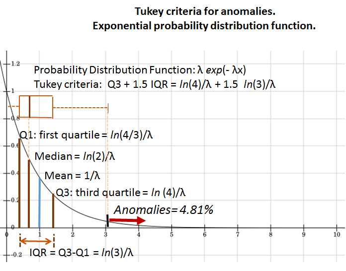 The natural solution, however, is to just use a second flip flop and make the synchronization process a synchronized chain. Our first flip flop might go metastable, but as long as it settles before the next clock edge sends the bit into the second flip flop, we’ll get a valid bit out of the second one. The probability of the state not settling before that edge follows an exponential distribution (see probability density function on the right - disregard text).
Once the bit comes out of the second flip flop, it’ll only change on the clock edge and be fully synchronous to the other parts of the MCU.
IDR v ODR
As you’ve likely come to realize by now, the GPIO is used for both input and output of the CPU. As such some components are specifically for the input, while others specifically for the output. Such is the case for the input data register (IDR) and the output data register (ODR). These aren’t the same component, and are used for completely different tasks.
The IDR is used for input. We saw that the Schmitt trigger is used to capture noisy voltage and put out a clean 0 or 1 that isn’t jittery. The subsequent flip flops (synchronizers) then take these bits and turn them into nicely controlled and timed logic states the CPU can work with. The following stop in for the incoming signals is then the input data register.
We’ve seen registers before in the CPU section, they’re essentially just a group of D flip flops sharing a same clock where the bit is stored in the latches. It might not seems obvious what the idea of an IDR is based on this, but essentially what it tries to solve is an architectural problem. The CPU cannot read random internal wires, such as the one coming from the synchronizers that changes every clock edge but isn’t part of anything. CPU’s instead read registers mapped into its address space.
Now what does “mapped into its address space” mean? Formally the address space is the set of all numeric addresses the CPU knows how to talk to. There’s a lot of these, and they’ll look like 0x00000000, 0x00000004, etc. Which has the idea that if the CPU wants data, instead of saying “give me RAM”, it just says “read from address X”, or “write value y to address Z”.
The output of this IDR is connected to the internal data bus. These buses, as we saw in the CPU section, are just wires connected together into metal routings. It’s what connects things, but at the same time it’s also a shared communication structure (with timing rules and so on).
Now this IDR has some great advantages. The synchronizer output isn’t architecturally visible, addressable by the CPU, nor timing guaranteed for the reading. This is all fixed by the IDR. The synchronizer ensures the incoming value is on the same clock timing, whereas the IDR ensures architectural visibility and bus protocol compliance.
ODR on the other hand works in reverse. When for instance the CPU wants to turn on the boiler enable, it cannot sit around and wait for it to happen while driving the wire. The CPU executes instructions and moves on. That’s the reason for the ODR, it’s a persistent state ensuring that the written instruction of the CPU is remembered until the output value has actually changed.
We again just have an array of flip flops clocked to the system clock and now written by the CPU over the bus. The bits that are written to it represent the level the GPIO output driver should attempt to attain. An important distinction from the IDR is that the driving of values in this case is software, not hardware.
The ODR feeds the output driver, which itself is either push-pull or open-drain, while also being either enabled or disabled by direction control. ODR stores the value while the driver applies it. Now it could be that the driver doesn’t apply it, for instance when the pin is still configured as input, or another component owns the pin at that moment, or a short occurs. There are many possible reasons for a mismatch between ODR instruction and output driver behavior.
Direction control
What remains now is some minor tying up of how various parts interact with each other. Direction control is about two independent decisions that take place after the MUX has selected GPIO as the owner of the pin. This “pin” I’m speaking of is one of those physical pins visible on the outside of the MCU (See CPU post). Such pins can have three states: Something outside the MCU drives it (button, sensor, etc.), the MCU itself is driving it (forcing high or low), or nobody drives it (electrically floating). The MCU is what chooses which situation applies at an moment.
This decision of the MCU is called direction control. We then want to know (1) whether the input path is enabled (CPU sensing the pin) and (2) whether the output driver is enabled (can CPU drive the pin). As such this direction control isn’t really part of the GPIO, other than in the way that it enables or disables input sensing and output driving.
These are kind of like two electrical switches controlled by one configuration decision. In software the decision is shown as a bit, 0 means input and 1 output. Physically, that pin is connecting two separate internal paths inside the MCU. There’s the input path where circuitry observes the pin voltage (Schmitt - synch - IDR) and then the output path where circuitry forces a voltage onto the pin (ODR - output driver - pin). That decision control decides which of these paths is allowed to touch the pin, electrically.
In input mode, the output driver is physically disconnected and the pin is configured as input. Pin voltage is determined by the outside world. So necessarily this means that if we’re in input mode, the output driver must be off.
In output mode, the output driver is connected and the pin is actively driven according to ODR. MCU is in full control over the pin. However, whether the input path is still enabled can vary by MCU.
Note that this decision takes the form of enable gates (remember the D-latch) on the input and output paths. This part exists solely to ensure clean separations.
Output driver type
In output mode the MCU is allowed to drive the pin, yet we haven’t really seen how this is accomplished. There are different ways in how to drive it, and this leads us to the driver types. There are different ones, because we sometimes want the pin either high or low, while at other times we want it to be pulled but otherwise left alone or just let something else decide what happens. As such we have push-pull and open-drain.
Physically, such a driver type is actually power hardware. Large transistors connect the pin to the power rail (VDD) or ground (GND) or nothing at all. This makes it the only part of the GPIO that can move real electrical energy as opposed to the decision making blocks we’ve been seeing.
The push-pull output is like a default version where the pin is actively driven high or low. There’s two transistors connected to the pin where one connects it to VDD (high) and the other to GND (low). Only one of them is then turned on at a time. If ODR = 1 the top transistor drives the pin high while if ODR = 0 the other drives it low. One pushes current out while the other pulls it into the pin. This output type gives the MCU full control with well defined pin voltage. It’s what we see when the LED blinks for example.
Open-drain output on the other hand will either pull the pin low or disconnect it entirely. There’s no transistor to pull the pin high. So we only have one transistor connecting the pin to GND (when ODR = 0) while nothing connects it to VDD. ODR = 1 then implies the transistor is off, and the pin is in a high impedance state (meaning it’s highly resistant). Something outside the MCU is then able pull the pin to high. Such disconnection can be quite useful, for instance when multiple devices share a wire, then open drain can let either pull the pin low but neither force it high.
Pull-up / Pull-down
We now get to solving some residual problems in the set-up. This GPIO pin is just a wire, and if we’re in a situation where for some reason neither the MCU or an external circuit is driving it, then the voltage on that wire is undefined. This implies that the wire is floating. It may pick up noise, go high or low, change based on randomness. We kind of want to prevent this because software has no way to reason in terms of maybe 0 or maybe 1. We again have a hardware problem that software cannot detect.
Remember that the GPIO has both an input and output mode, and in input mode the MCU is reading the pin but not driving it (the output driver is off). When input mode is active, we therefore want to ensure that we see a predictable default value even though nothing is happening necessarily. The pull-ups and pull-downs exist to ensure that we get a sort of default value whenever no one is driving the pin.
Physically, we have a resistor connected inside the MCU between this pin and either VDD (pull-up) and GND (pull-down). Such a resistor has quite high resistance (e.g. 50 kΩ), so it provides only little current to the pin and doesn’t really put up a fight for real drivers such as the push-pull output. If we look at Ohm’s law (I (current) = V(volt)/R(resistance)), then with typical values in our senseo case, we have 3.3V and 50kΩ internal pull-up resistance which implies a current of 66 µA. Meanwhile the GPIO push-pull driver pulls low with some 5 mA (thousands of µA).
If pull-up is enabled, then if nothing else drives the pin it will be read as high while if something else pulls it low, it’s read as low. This path is the reason buttons are often wired to GND, since that means that if they’re untouched, the pin floats and the pull up makes it high, while if pressed the button connects to GND and low wins.
If pull-down is enabled then the pin reads low if nothing else is driving it while high if something else drives it high. We here have a default low. With these pull-up and pull-downs we simply have bias sources for the pin. They’re most important for the input mode or for the open-drain output type, as then we have possibility of floating behavior.