Senseo GPIO Button Example
This post is part of the Senseo series:
- Senseo Prelude
- Senseo Electricity Basics 1
- Senseo Electricity Basics 2: Generation
- Senseo Electricity Basics 3: Grid to Wall Socket
- Senseo Boiler: Heat and Electricity
- Senseo Boiler: Sensing Temperature
- Senseo Boiler: Sensing Temperature Part 2
- Senseo Boiler: Safety
- Senseo Boiler: Brewing
- What is Plastic?
- PCB - Printed Circuit Boards: Fundamentals 1
- PCB Fundamentals 2: MOSFET Transistors
- PCB Fundamentals 3: CMOS Logic
- PCB Fundamentals 4: Combinational v Sequential Logic
- PCB Fundamentals 5: D-Latch
- PCB Fundamentals 6: Clocks & Flip-Flops
- PCB Microcontroller Subsystems: CPU core
- PCB Microcontroller Subsystems: GPIO
- Senseo GPIO Button Example
- PCB Microcontroller Subsystems: ADC (Conceptual)
- Senseo Interlude: Considering Quality
We’re now in the perfect place to briefly explore something on the side, apart from the intricate MCU electronics. With the tactile switch, we found the object that connects a whole bunch of machinery.
Tactile switches
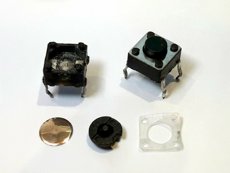
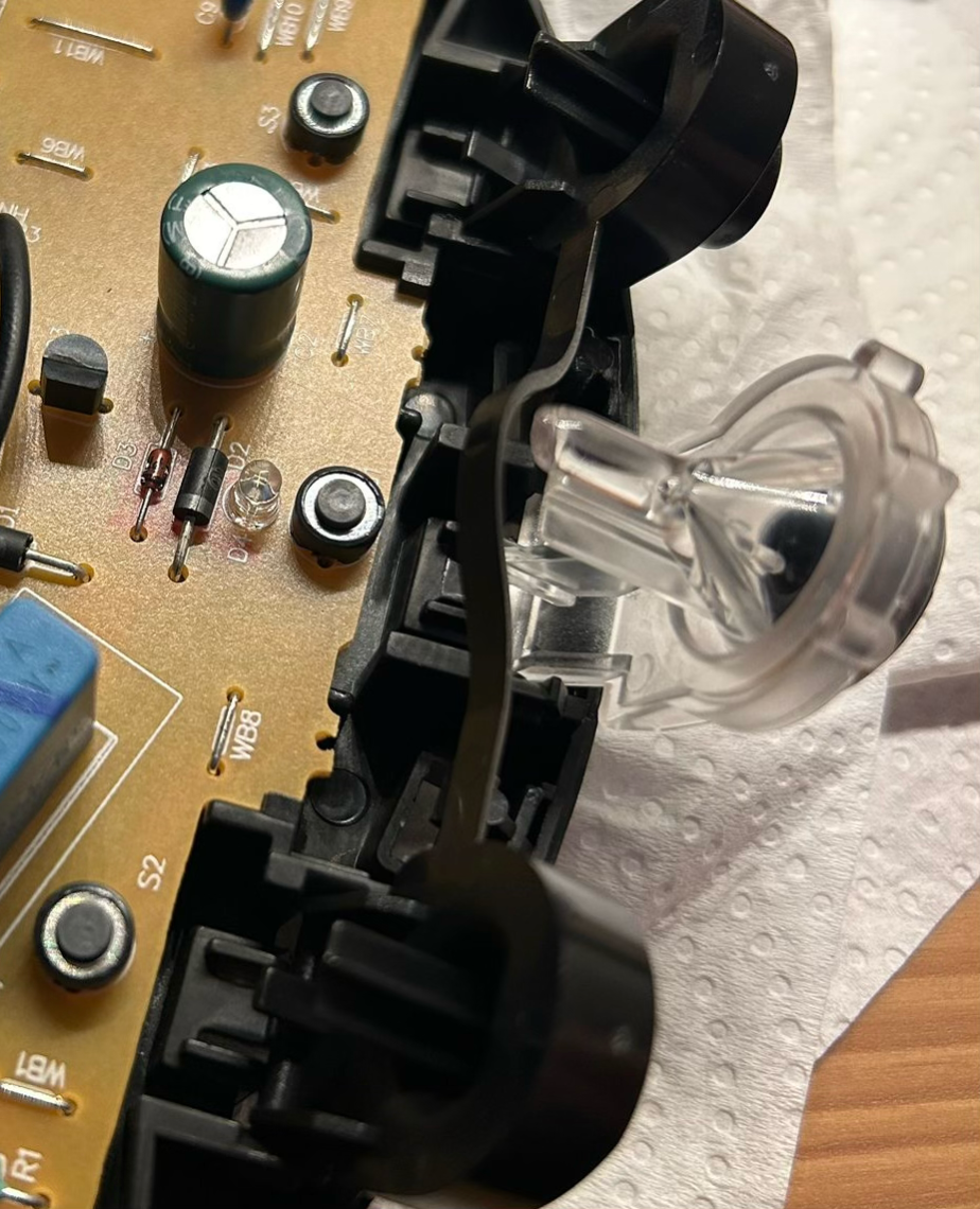 What we see on the PCB, right where the buttons touch down, are small tactile switches. These are cleverly connected to the buttons we press, but seeing it like this makes it obvious that the button are merely lying on these switches waiting to be pushed in.
The tactile switch itself is a small plastic case with a moveable metal dome in the middle. This is then covered by a little button cap (black). In the picture down below from wikipedia you can see the disassembled button, as well as the plastic casing and cover and metal dome. What then happens is when we press the button, the metal is pushed down, onto two metal contacts. If you look closely at the inside of the disassembled switch, you can actually see these two touching point left and right.
The idea is that in resting position, the metal dome sits slightly above the contacts, and so the two metal pads/contacts aren’t connected. When we then press the button, the metal dome is pushed down, and connects the metal pads. It isn’t actually pushed down, it remains fixed in the same position, but it bends in the middle to arrive at the same result.
The two wires connecting two sides of this button and coming to the metal pads are then connected, and electricity can pass. Essentially a circuit becomes connected. The reason the dome is metal is also because it conducts electricity quite well.
It’s actually a very intuitive design, when pressed down it bends and flips downwards, connecting the two points. Then when we release, there is a snap back and the metal dome comes of the metal contacts. This snapping is nothing more than a clever way to let the user know the button was pressed.
The next question would then be what the wires are on either side of the switch. I mean, where do they come from, and why is it okay for them to remains unconnected from anything? The most straightforward way to reason about this is by looking at electricity basics.
We may have voltage on the wire coming in on one side at all time, while the other wire leads to ground (the reference). When the button isn’t pressed, there’s no closed loop and no current can flow. The button wire then sits at 3.3V and the MCU reads this as button being high, and therefore not pressed. Meanwhile when the button is pressed, the two sides connect and current flows to ground node. The voltage of the button wire therefore goes to 0V, which the MCU reads and interprets as button being pressed.
Power
To get ourselves a cup of coffee, we must first power on the machine. From the visual from before, it’s the big and almost transparent button in the middle. It even has the little LED light right above it.
The power button is a little special compared to the brewing ones, since the reality is that there is likely a very small circuit inside the machine that is powered at all times. In standby mode (off), this circuit is powered and the MCU most likely has some partial control. This way, when we press the button, it actually exactly the same mechanism as explained before. There is 3.3V on the wire coming to the button, and the other wire of the button leads to ground. Once pressed, the current flows and the button wire get a brief 0V.
The MCU (being half awake) is able to read this signal and takes this as instruction to turn everything on. That’s why when we press the button, lights start blinking, water level is being read, and the boiler starts heating.
GPIO
It’s not like the MCU is able to directly read what’s going on, though. The button is pressed only for a second, and what happens is that the press briefly causes a current flow to ground (0V). This causes a change in magnetic field that ripples through the wire at close to the speed of light. The signal is then picked up by the GPIO (the wire was at high voltage as a result of the pull-up we saw at the end of the GPIO section).
More precisely, it arrives at the GPIO pin, where the the input buffer ensures that the duration or the force of our press on the button doesn’t signal multiple or messy information. The brief 0V field arrives at the input node of the Schmitt trigger (assuming the outdated version with resistors I used as example). This leads to our canonical case where input was falling. NMOS will then taper off while PMOS gradually turns on (depending on how clearly we pushed the button - though for buttons this isn’t too big a problem given the switching mechanism).
But remember, the node between VDD and PMOS on the Schmitt was pulled lower because a feedback PMOS transistor (controlled through output which was high) is pulling it to ground. As a result, the source of the real PMOS is pulled lower than it otherwise would be, and the input needs to go beyond a certain threshold to fully ensure output is pulled to high.
So our button press, which caused a brief signal of 0V, arrived at the input buffer, where the signal was standardized, and the output was turned to 1 (or high V). That’s because the input was low, but this is a sort of inverter, so the output reading of the Schmitt trigger is high.
After, this signal goes through two flip flops to ensure synchronization with the clock edge. This is achieved because our signal, which is 1 bit, has now come from the Schmitt trigger and arrives at the flip flop through the D wire (its input). Meanwhile, the enable ‘gatekeeper’ as I like to call it is attached to the same clock as the MCU. So the signal must wait for the clock edge to be able to enter the first flip flop.
This isn’t a problem and the signal won’t be overwritten during its wait, because the clock edge happens every 10-100 ns while the signal is likely some 1-10 ms long. Nevertheless, if anything goes wrong with the signal and metastability ensues, the second flip flop will straighten this out.
Perhaps a little recap on the flip flop design. We have two D-latches connected to one another, which are cross coupled inverter gates with a transmission gate on. The cross coupled inverter is what provides the storage of memory, through input an output being interconnected. The transmission gate is two transistors (PMOS and NMOS) where NMOS’ gate is attached to what’s called the Enable wire (in our case the clock edge), and PMOS to the opposite of the enable wire (actually the same wire but with an inverter in-between). This ensures that when the clock edge happens, both PMOS and NMOS are conducting. Both PMOS and NMOS are used because the one passes strong 1’s and the other strong 0’s.
So our signal came from the input buffer, and is active on the D-wire of the flip flop’s first latch. Meaning the wire is pulled high because of the signal. The enable wire is pulled high through the clock edge, and so the transmission gate conducts. The signal enters the cross coupled inverter, where it can remain. But we’re not just in a D-latch here, we’re in a flip flop. And a flip flop has two D-latches connected to one another. The second D-latch’s D wire is actually just a wire coming from the output of the first latch. But here, the enable wire is made the opposite of that of the first latch, so that if the transmission gate of the first is conducting, that of the second is not. As such the signal can never just pass through the latches. Only one transfer happens per clock edge.
And so after some clock edges, the signal of our button press has passed through both flip flops required for synchronization. It’s perfectly synchronized now with the rhythm of the CPU internal world.
After, the signal enters the Internal Data Register (IDR), which was just a bunch of such flip flops attached to one another. It exists to solve the issue that the CPU cannot read standalone wires, and instead reads registers mapped into its address space. This address space is set up through memory, which we’ll see later on. The signal is now completely ready to be picked up by the brain of the Senseo.
CPU
We’ll come back to this once we’ve dissected the flash memory.