PCB Fundamentals 5: D-Latch
This post is part of the Senseo series:
- Senseo Prelude
- Senseo Electricity Basics 1
- Senseo Electricity Basics 2: Generation
- Senseo Electricity Basics 3: Grid to Wall Socket
- Senseo Boiler: Heat and Electricity
- Senseo Boiler: Sensing Temperature
- Senseo Boiler: Sensing Temperature Part 2
- Senseo Boiler: Safety
- Senseo Boiler: Brewing
- What is Plastic?
- PCB - Printed Circuit Boards: Fundamentals 1
- PCB Fundamentals 2: MOSFET Transistors
- PCB Fundamentals 3: CMOS Logic
- PCB Fundamentals 4: Combinational v Sequential Logic
- PCB Fundamentals 5: D-Latch
- PCB Fundamentals 6: Clocks & Flip-Flops
- PCB Microcontroller Subsystems: CPU core
- PCB Microcontroller Subsystems: GPIO
- Senseo GPIO Button Example
- PCB Microcontroller Subsystems: ADC (Conceptual)
- Senseo Interlude: Considering Quality
 At the end of the sequential logic section, we saw the SR latch and how it provides a way to overwrite memory created by cross-coupled inverters. Now the problem is that such an SR latch is quite messy as it’s difficult to manage. For instance, it has a forbidden state resulting in undefined behavior when S=1 and R=1, it introduces quite a few wires, and given our two nodes S and R slight mistiming between the two results in glitches. The two big practical problems are essentially that we have too many control signals (S and R) and no control over when memory updates.
Because of these, the D-latch was introduced with just one data input (D) (and one enable signal (EN) controlling when D is connected). Again we have the core of memory, two CMOS inverters cross-coupled to each other to create feedback. As such we have memory, but not yet control. What’s really needed to have control is finding a way to temporarily overwrite feedback and then letting it hold again. This is done by connecting the input D to the memory node only when we want it to.
Remember on the cross coupled inverters that we have our output node now called either Q (which feeds B’s input) or Q̅ (which feeds A’s input). Such cross coupled inverters have memory and will always have two possible stable states, Q=1 and Q̅=0 or vice versa. It remembers even when input is gone, but it’s also sealed off from the world. It’s a very intuitive way to actively memorize a bit of information. For the SR latch to work, we then connected additional transistors onto Q and Q̅ such that when S or R turned on, the node yanked back to ground V. However, we now don’t want to overpower anymore, we simply want to disconnect it.
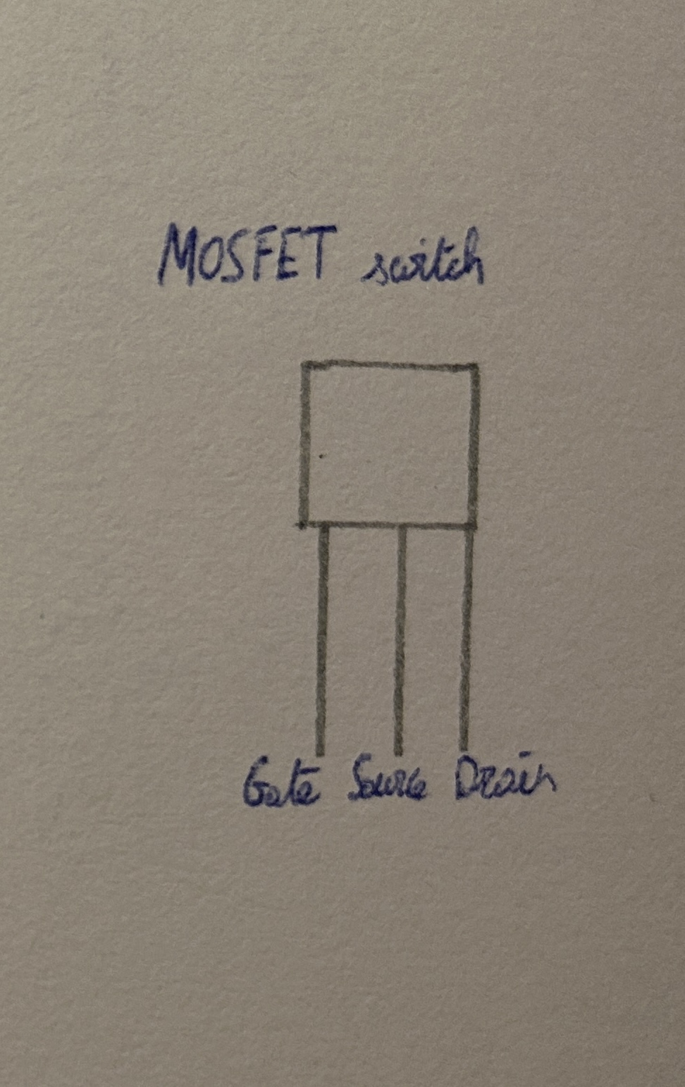
That’s where the transmission gate is introduced, which is really just one NMOS and one PMOS placed in parallel: Input (D) - NMOS = PMOS - Output (X ~ the input of the inverter). What’s important to realize is that we here don’t talk about a logic gate but instead a bidirectional switch. We need both an NMOS and a PMOS gate in parallel because NMOS passes strong 0 (weak 1) while PMOS passes strong 1 (weak 0). In terms of control, we then have EN = NMOS and ¬EN (not EN) = PMOS, where ‘EN’ refers to ‘enable’. EN = 1 signifies that both of these transistors are on and implies that the input gets connected to the output. Now what I meant with ‘bidirectional witch’ is that unlike a logic gate that drives output by interpreting voltage, a transmission gate doesn’t decide anything but merely connects two nodes together. There’s no VDD and GND, only the input wire D and the output connecting to the input of one of the inverters.
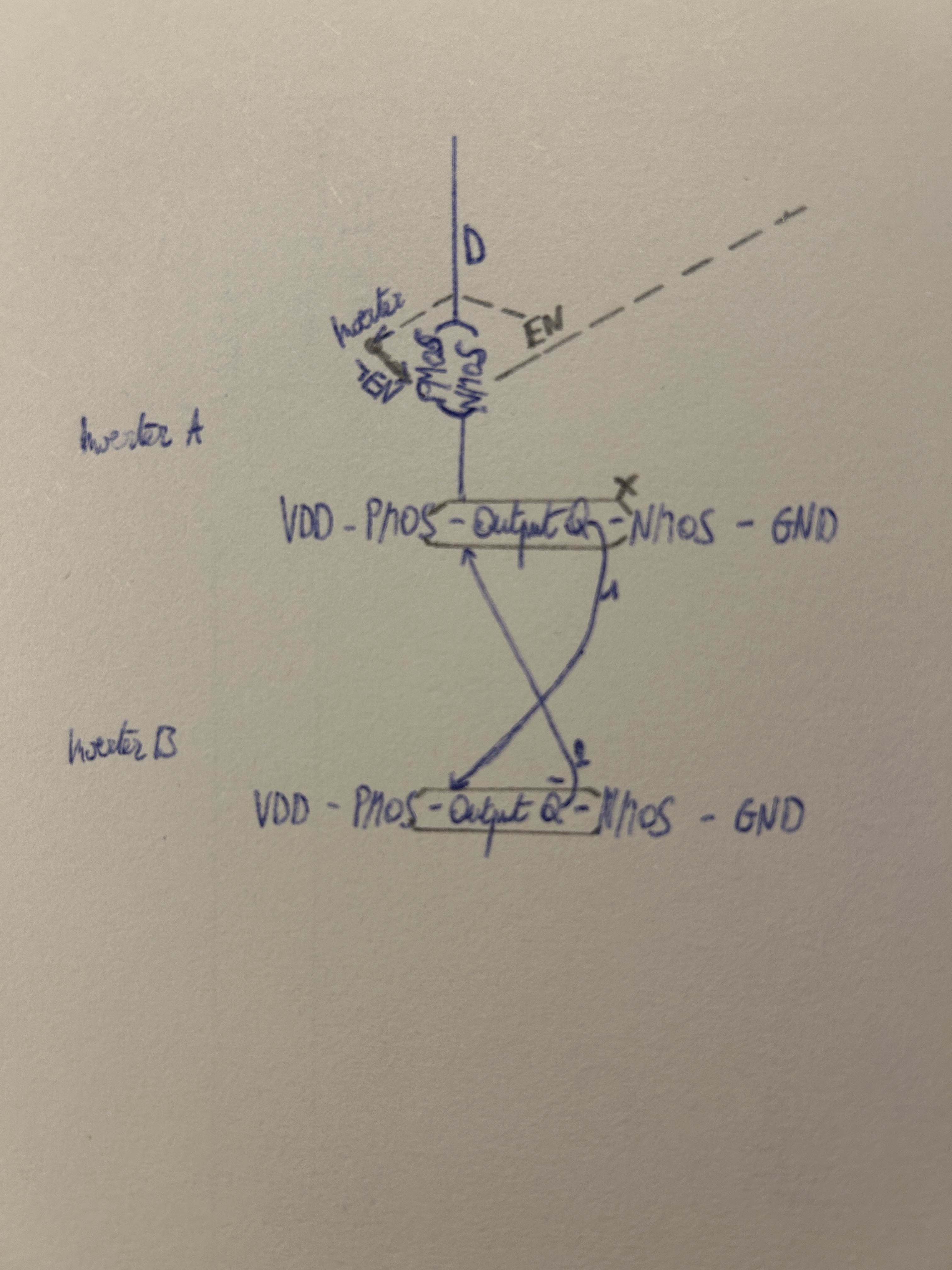
So we now have an input D that’s able to write the stored value but only when we enable it. The cross-coupled gates are left alone otherwise. D is connected via the transmission gate to the input node of one of the inverters, thereby influencing Q. EN’s state, meanwhile, is influenced usually by the clock signal, which we’ll see later.
Let’s say EN=1, we then have both transistors in the transmission gate on and D physically wired to the inverter’s input. D directly drives the inverter input, inverter A in turn drives Q, which in turn drives inverter B and at last Q̅ feeds back. When D changes, the storage node Q is charged or discharged (depending on D’s value) and the feedback loop reinforces the new value, which is then remembered. When EN=0, there’s simply feedback as was before.
In practice, D is already a CMOS-driven node, as it’s usually a wire coming from another output (logic block, another latch or flip flop). It’s therefore actively driven high or low by other transistors.
Again, this EN is the wire for the NMOS, while PMOS has an input wire called ¬EN (not EN), which is then actually just a wire coming from NMOS’ EN but with an inverter attached to it.
Now it’s all about threshold voltages in the end. When EN=1, the transistors are on and the transmission gate behave like a low resistance wire between D and X, meaning that If D is high and X low, charge flows from D to X until equal, while the other way around is equally possible (though less likely). That’s where ‘bidirectional’ comes from, current is allowed in both directions depending on which side has higher potential (see the aside below).
On a visual portraying the conduction paths, this will never come through, but it’s a very important part to see and understand. The view we must then get is that with this memory block (2 cross couples inverters - or NAND, or NOR gates), we have that inverter A’s output has a wire going to the input node (1 single node) of inverter B. This input influences B’s output, where a wire goes to A’s input node. Then at A’s input node X, we have both this wire coming from B’s output, but also a connection to D via a transmission gate. This transmission gate is then again a PMOS and NMOS, whose drains are attached to a wire which attaches to input X. These two inverters are parallel and their sources (source and drain are interchangeable here) are both attached to wire D. The enable EN wire comes from a clock and goes to NMOS’ gate pin, but also gets attached a very small inverter and goes to PMOS’ gate pin. There’s no shortcut because neither is attached to VDD or GND. That’s the full picture here.
Aside on threshold-loss in transmission gate:
Now there’s been a question on my mind when going through this, which is why we need both PMOS and NMOS in the transmission gate, and sure I answered this saying the one passes strong 1’s and the other strong 0’s, but truly why is this? The answer to this lies in the inner workings of how these CMOS transistors work (as already partly detailed before), which is essentially through threshold logic. To explain this, I must explain some of the names used:
External power related:
- VDD: the positive supply voltage of the chip (often DC 1.2-5V)
- GND: ground reference of the chip (0V)
Node voltages (measured against GND):
- VG: voltage at gate terminal of MOSFET
- VS: voltage at source terminal
- VD: voltage at drain terminal
- VA: voltage on input node (on the transmission gate, this is D coming in)
- VB: voltage on output node (“, the wire attached to output node of inverter)
Derived voltages (difference between terminals):
- VGS = VG-VS: voltage difference between gate and source (control voltage for NMOS)
- VSG = VS - VG: same exact idea but for PMOS
- Vth: a threshold voltage, which is a device property (between 0.3-0.7V) and is the minimum gate to channel voltage needed to sustain a conducting channel. Comes from the doping process and thickness of the oxide.
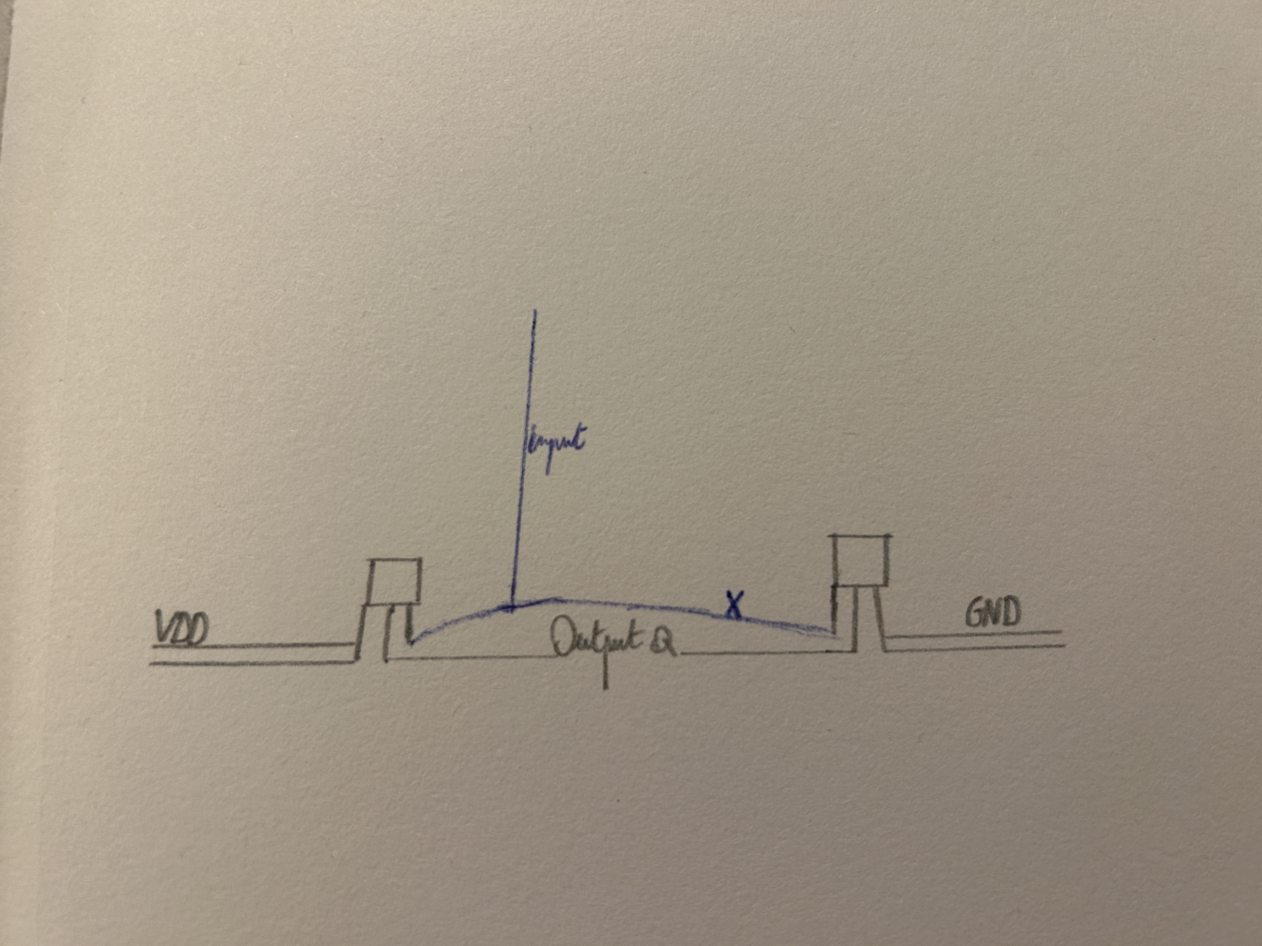
Now that this is clear, we can see how a MOSFET switch truly turns on for pass transistors such as in the transmission gate. Caveat here: for the logic inverter with transistors on it, nothing about this threshold-loss applies in a problematic way which is why we just need NMOS for pull-down and PMOS for pull-up.
For such a pass NMOS for instance, its source and drain are attached to input (D) and output (where its output is actually attached to the input of the inverter), while gate is attached to the Enable signal. To be clear, it isn’t attached to power, but we say that if the transistor is fully on, EN = 1 and therefore EN ≈ VDD. So we say VG = VDD even though it’s not truly attached to VDD.
For NMOS in the transmission gate to turn on (remember NMOS = 1 if input 1), the voltage difference between gate and source (VGS) must exceed threshold voltage. Now in the scenario where VA (D) is high (1), we see that just like we said above, VA is supposedly equal to VDD. In such a case, VA = VDD and VG (gate) = VDD. As a result, VGS = VG - VB (VS) = VDD - 0 and VGS is as such above the threshold voltage of 0.3-0.7, as it’s fully 1. Now in the course of time because NMOS is on, charge flows from A to B which raises VB (output), such that VGS = VG - VB = VDD - VB. As VB increases (by current flowing to B) VGS decreases and eventually VGS = Vth. When this occurs the channel can no longer be sustained and NMOS turns off. This is what is meant by saying NMOS passes weak 1 in the above explanation on transmission gates. This doesn’t occur to the inverter, as there the NMOS is fixed to GND so the output cannot approach VG and consequently NMOS never passes high voltage.
That’s why we need both PMOS and NMOS in this transmission gate. Because the enable (EN) signal also goes to PMOS (with an inverter on it so it becomes ¬EN), it gets the exact same signal as NMOS, i.e., when EN turns on, PMOS and NMOS both turn on (as PMOS requires low input to turn on). In the case of passing logic 1: VSG = VS - VG where source is at VDD (1) and gate at 0 (when turned on and conducting): VSG = VDD - 0 = VDD, but as X (PMOS’ output, inverter’s input) rises towards VDD because current is conducting, the gate stays at 0 and VSG always stays large. The channel can therefore never collapse and PMOS always passes full 1 (VDD).
Passing logic 0: D=0 and because in such a case we want to overwrite the memory, X is naturally at VDD in this scenario. Now with PMOS, as gate = 0 when on, VSG = Vx - 0 as X falls and we’ll see the channel collapse when Vx ≈ Vth. So PMOS alone is weak 0. Meanwhile NMOS in this case has gate at VDD and as X falls (VGS = VDD - Vx) we see VGS increasing, so NMOS will pass strong 0. It might be confusing to read ‘as X fall’ but contrary to the pull-up/down transistors in the logic gates, a pass-through transistor such as in the transmission gate merely conducts. Depending on which side of the transistor has higher potential, current can flow in either direction when they conduct. So when transistors are on, X (transistor input) is high (1) while D low (0), current full flow from X.
But again, even the D latch isn’t perfect as it fixes correctness but not coordination. Once we scale up for large systems, we usually have it so that latch 2 is attached to latch 1’s output, latch 3 to latch 2’s output and so on. Now the problem is that when EN = 1, the latches behave like open doors and are essentially ‘transparent’. In such state, a change in D1 (attached to latch 1) will propagate through the latches as long as EN stays on (= the race through problem) and this also happens if D goes to 0 within the same EN window. Designers usually want a single EN cycle to just cause one latch to change, but instead they have as many latches impacted as the signal can pass through before EN goes low. Because of this, behavior of the latches depends on transistor speed, temperature, supply voltage and so on, such that it might work on our desk but fail in a different environment. As a result of this racing through, we can also not tell where the data resides at any one moment, it might be stage 2 or stage 4, but we don’t know. We’ll now see how clocks and flip flops answer this problem, where clocks are shared timing signals that tell all memory elements when they’re allowed to update so that changes happen in a coordinated way instead of continuously. The flip flop is then a memory element (like the d latch) which is built to listen to the clock only at a specific instant so that data moves exactly one step at a time and never ripples uncontrollably through the latches.