PCB Microcontroller Subsystems: RAM and FLASH memory
This post is part of the Senseo series:
- Senseo Prelude
- Senseo Electricity Basics 1
- Senseo Electricity Basics 2: Generation
- Senseo Electricity Basics 3: Grid to Wall Socket
- Senseo Boiler: Heat and Electricity
- Senseo Boiler: Sensing Temperature
- Senseo Boiler: Sensing Temperature Part 2
- Senseo Boiler: Safety
- Senseo Boiler: Brewing
- What is Plastic?
- PCB - Printed Circuit Boards: Fundamentals 1
- PCB Fundamentals 2: MOSFET Transistors
- PCB Fundamentals 3: CMOS Logic
- PCB Fundamentals 4: Combinational v Sequential Logic
- PCB Fundamentals 5: D-Latch
- PCB Fundamentals 6: Clocks & Flip-Flops
- PCB Microcontroller Subsystems: CPU core
- PCB Microcontroller Subsystems: GPIO
- Senseo GPIO Button Example
- PCB Microcontroller Subsystems: ADC (Conceptual)
- Senseo Interlude: Considering Quality
- PCB Microcontroller Subsystems: RAM and FLASH memory
Memory (flash and ram)
We’ve referred before to the notion of “instructions coming from memory,” and it being used in the CPU to handle the peripherals. Think for instance about the size of a single cup of coffee. Somehow the machine must know how many ml must be pushed by the pump through the boiler, through the pad and into the cup.
This is where the programmers at Phillips come in and provide instructions.
We have then both Flash memory and RAM (likely Static RAM in this case). The former refers to the actual program memory while the latter the a working memory. Both are needed and serve very different purposes.
General RAM (Random Access Memory)
Since we’re uncovering topics about the Senseo that are practically unknowable except on the conceptual level, we mustn’t let that hold our curiosity back on how these components work.
As might have been expected, a core tool for memory is the D-latch, those cross coupled inverters where a D wire is attached to one of the inverters and overwrites when the enable signal on the transmission gate allows it (clock controlled).
Such a latch stores 1 bit, which has value 0 or 1. And since it’s not directly influenced by what happens on the input, but holds its state except when the enable signal allows the D wire to overwrite, we have memory.
It is then possible to place 8 such latches together, and get a Byte. Bytes are generally quite important because by placing 8 latches with each 2 possible values together, there’s a total of 2^8 = 256 possible combinations. This might seem like a random number but it’s the perfect number of combinations to facilitate the English language and punctuation. So that’s how it came into existence historically, but it isn’t the main use for RAM.
With RAM we have many such bytes (possible 8 bit combinations like 10110100) and each of these is an address. And address that can be written to (and read) by the CPU to temporarily hold information while the machine is running. As such it’s a volatile memory, because once the machine is turned off, the ‘memory’ is erased, and hence the difference with what we’ll see with flash memory.
So now a ton of address locations can exist, but the way the CPU has access and does anything useful with these bytes is through a decoder. This decoder basically bridges the physical location of data and the desires of the CPU.
When we press ON for a cup of coffee, the CPU will note the demand, and put that into the RAM to remember while doing all the other stuff like heating water. The programmer will have chosen a certain address to hold the meaning, and the decoder therefore reads the input from the CPU and selects automatically the correct address. Then later when the water has warmed up, the CPU goes back to that address line and reads the desired actions, as it doesn’t remember by itself and is merely doing tons of little calculations at any given time. This RAM is used for storing temporary values such as current water temperature, tracking pump running time and so on.
This decoder is further just combinational logic, which we’ve seen before. Essentially the decoder behaves like a switch that, given the information coming from the CPU, automatically selects the appropriate address. With the data input coming from the CPU, this is then written to that address, and can later be read again.
They here seems to be that there is a physical layout that supports reading. Nothing is by itself intelligent enough to be “reading” or “writing” something. It’s all through transistor switches, which are combined through latches, combinational logic and so on, so as to behave the way the designer wants it to when the operator performs one of the fixed and known actions.
The name random access memory is then simply originating from the combinational logic nature of the decoder, namely that any address can be accessed in roughly the same time. There’s no sequential order going on, but selection of addresses is instead purely dependent on what happens at that moment, and as such there’s no time difference between selecting address 1 or address 3,000,000.
And so to recap: the CPU notices that a certain action has been set in motion (such as power on), and so will store the request in the appropriate address, while rapidly looping through the program written by the designer (in flash memory), whereby it checks temperature, water level, and so on, and once all is ok, it reads again from that address and moves on to the next step. This next step for instance is the constancy of the light of the power button, indicating that the water is heated enough to choose a cup size and pour the coffee.
Flash Memory
Now with the flash memory, the story revolves around memory that doesn’t get erased the moment power is out or the machine is off. This is quite essential because it ensures that the correct program is executed, that the CPU loops through the correct sequence, gets the temperature to the exactly right temperature or how long to run the pump so as to have the exact right amount of water being pushed through the head. It even ensures that every machine has the same uniform way of blinking lamps.
Essentially the RAM was like a whiteboard, while the flash is like engravings in stone, which are still there after years with no power. In this way the main instructions of the machine can be stored at production, and from then on the CPU can just loop through these instructions and apply them. It’s then the true driver of everything happening the way it does. The main component here is called the floating-gate transistor.
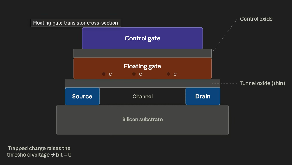
These are a special type of MOSFET designed to hold a value forever. As can be seen in the visual, there is a sort of isolated material within the gate part. This is then floating because it’s not connected to any wire, and whereas the regular MOSFET has a gate, source and drain, we here have a second gate between the regular gate and the channel that’s in-between layers of insulated material (the silica we mentioned before).
The way the designer gets this floating gate to hold a certain value (e.g. 1) is by connecting wires to both control gate and drain (or source), and applying voltage on both. Electrons then accelerate in such a way that some will get trapped in the floating gate. And the way this transistor consequently works is that the floating gate holds more electrons than it usually would, therefore being more negatively charged, and as such the threshold for creating the channel changes.
So a floating gate transistor will need more charge applied to the (control) gate in order to have a channel between source and drain. This is the key feature because the floating gate has no wire attached, and hence there’s no direct way to measure its value. By applying a voltage to the transistor (control gate), and seeing whether its channel turns on, we can detect whether the floating gate had a 0 or a 1.
And this really stems from the fact that if the floating gate is uncharged (0), the threshold isn’t changed and a voltage applied to the control gate will turn on the channel. Meanwhile if the FG is charged, the threshold changes and applying charge to the control gate won’t create the channel.
Now we know the core component - floating gate transistors, but need to connect it to the bigger picture for the flash memory. This is again a difficult task because there’s no public information on what kind of flash memory Senseo uses. It likely isn’t NAND flash such as phones and laptops use, but much simpler.
Imagine that we have 4KB of flash memory, that means we have 4 times 1024 bytes where each byte represents 8 bits. These bits are the floating gate transistors reading either 0 or 1 (that’s actually 32k+ transistors for that flash memory). And that’s then how those instructions are encoded by the designer.
For instance the following bytes can represent the adjacent instructions (only us humans have value for - the transistors just present what they present, and the CPU interprets them in mechanical manner) for temperature checking:
- 10110101 — “load the value from this address into the working register”
- 00110001 — “compare it against this threshold”
- 11000010 — “if less than, jump to this address”
As such combining bytes can lead to instruction sequences that the CPU reads and performs the cycle.